
This is a translation of a foreign article, so there may be inaccuracies.
https://www.avpasion.com/oled-transparente-electrodo-invisible-conductor/
Major Breakthrough in Transparent OLED: Korean Researchers Successfully Develop High-Conductivity Electrodes That Are Barely Visible
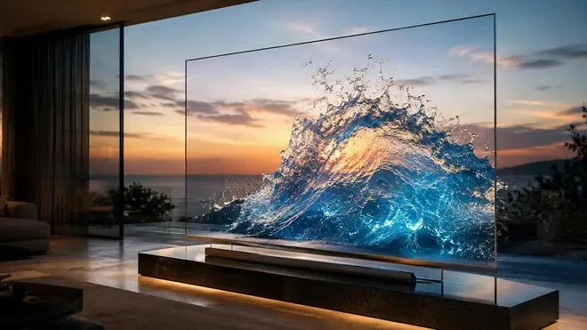
Transparent OLED, which has been discussed for years as a technology that seemed straight out of futuristic movies, is gradually becoming a reality. It's not just limited to unique display TVs for exhibitions, but extends to automotive displays, augmented reality (AR), smart storefronts, information-integrated windows, and even flexible devices.
As with these technologies, the challenge isn't simply making the screen look good. The material must be transparent while also conducting electricity well, and the manufacturing process must not damage the organic layers of the OLED. And this last part is a far more difficult and delicate task than one might think.
In this context, a research team from Seoul National University's College of Engineering, led by Professor Hong Yong-taek, has announced a very powerful technology. A transparent OLED top electrode based on highly conductive metal mesh, fabricated using metal-selective deposition technology. While it sounds like highly technical jargon, the idea is simple: to allow electricity to flow without blocking light and without damaging the panel during manufacturing.
The Real Challenge of Transparent OLED Is More Than Just Making It Transparent
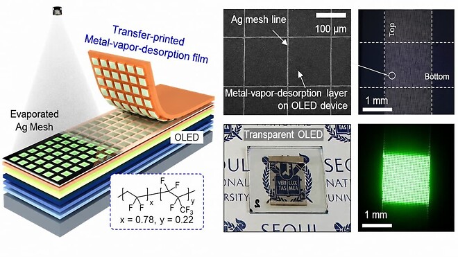
Inside typical OLEDs, there are many chemical and electronic mechanisms hidden. However, with transparent OLEDs, light must be emitted in both directions, and the top electrode must not act as an opaque cover, making the structure much more complex. It must be transparent enough to allow images to pass through while being conductive enough to ensure the device operates at peak performance.
Many transparent electrodes have managed to perform one function, but often fail when directly integrated onto OLED. This is because some manufacturing processes require steps that can damage the underlying organic layers, such as chemical cleaning or lift-off. In the OLED field, this is a very dangerous element because it deals with very sensitive materials.
The solution devised by this excellent research team is a high-resolution transfer technique using a layer called MVDL (Metal-Vapor-Desorption Layer). With this method, micrometer-scale metal patterns can be formed directly on organic structures without aggressive processing. In other words, it draws a very fine metal mesh on OLED without damaging the underlying structure.
Metal Mesh with Up to 99% Transparency and Very Low Resistance
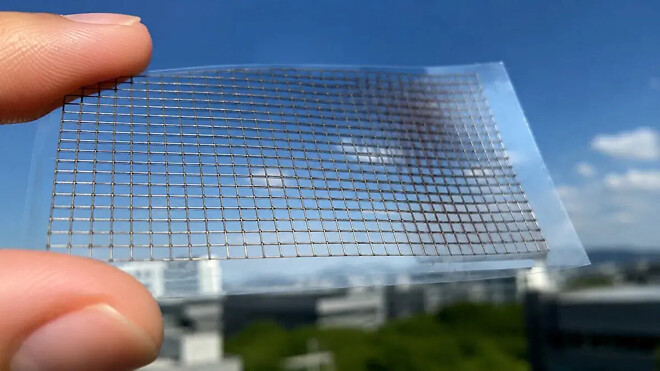
The published data is quite noteworthy. The fabricated electrodes achieved optical transparency between 93% and 99%, with sheet resistance of only 1.1 to 4.0 Ω/sq. For those unfamiliar with this field, lower sheet resistance means better conductivity of the electrode. And higher transparency means less visual interference.
The research team also reported achieving a Figure of Merit of over 10,000, an exceptionally high figure for a transparent electrode less than 1 micrometer thick. This means the material is not only transparent for the sake of looking good in a demo, but has very serious and excellent electrical performance.
The impressive part is that they didn't stop at just fabricating the electrode. They actually implemented a transparent OLED using the metal mesh as the top electrode and demonstrated that it maintained excellent transparency and high electroluminescent performance without degradation of the internal organic layers. The key point is that these numbers are maintained even when the technology is applied to actual devices.
This Doesn't Mean a Perfect Transparent TV Will Come Out Tomorrow, But It Points to a Massive Direction

These advances won't lead to commercial TVs overnight, so some realistic clarification is needed. However, they align perfectly with the industry trend of wanting thinner, more flexible displays that integrate into everyday objects or are completely transparent.
Professor Hong Yong-taek explains that through this process, not only can high conductivity and high transparency be achieved simultaneously, but fine patterns can also be formed directly on organic substrates. This will open doors to very interesting applications, ranging from transparent flexible displays and optoelectronic devices to panels linked with facial recognition.
This research was published in the scientific journal Materials Horizons and was selected as the cover paper (Outside Front Cover) of that issue. This shows that it is no light achievement. I believe that even if this doesn't receive as much attention as new TVs boasting brightness levels of thousands of nits, it is one of the advances that will ultimately hold tremendous significance in the future to come.
While transparent OLED still has a long way to go, these combined research efforts bring us closer to a future where displays are invisible, flexible, and blend much more naturally into our daily lives.